- Español
- Português
- русский
- Français
- 日本語
- Deutsch
- Italiano
- Nederlands
- Polski
- 한국어
- Svenska
- magyar
- Malay
- বাংলা ভাষার
- Dansk
- Suomi
- हिन्दी
- Pilipino
- Türkçe
- Gaeilge
- العربية
- Indonesia
- Norsk
- تمل
- český
- ελληνικά
- український
- فارسی
- български
- Latine
- Azərbaycan
- Македонски
- Lietuvos
- Eesti Keel
- Română
- Slovenski
- Srpski језик
- 简体中文
- Català
- שפה עברית
- беларускі
- Frysk
- ગુજરાતી
- ಕನ್ನಡ
- Kurdî
- Gàidhlig
- Тоҷикӣ
- O'zbek
- Lëtzebuergesch
Products
- View as
-

-

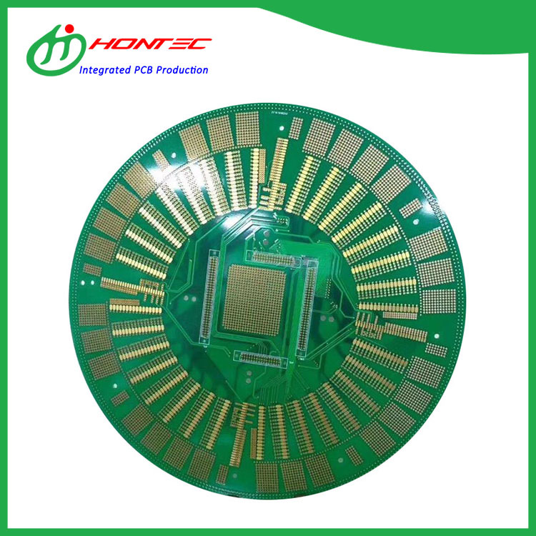
IC Test PCB
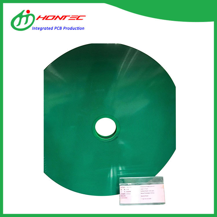
Any integrated circuit is a monolithic module designed to complete certain electrical characteristics. IC testing is the test of integrated circuits, which uses various methods to detect those that do not meet the requirements due to physical defects in the manufacturing process. sample. If there are non-defective products, the testing of integrated circuits is not necessary.The following is about IC Test PCB related, I hope to help you better understand IC Test PCB.
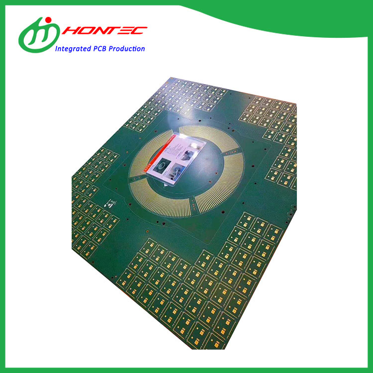
Read MoreSend InquiryEM-890K PCB
IC testing is generally divided into physical Visual Inspecting Test, IC Functional Test, De-Capsulation, Solderbili, ty Test, Electrical Test, X-Ray, Rohs and FA.The following is about Large size EM-890K PCB related, I hope to help you better understand Large size EM-890K PCB.
Read MoreSend Inquiry10-Layers Coil PCB
10-Layers Coil PCB--The coil usually refers to a wire winding in a loop. The most common coil applications are: motors, inductors, transformers, and loop antennas. The coil in the circuit refers to the inductor.The following is about 10 Layer Oversized Coil Board related, I hope to help you better understand 10-Layers Coil PCB.
Read MoreSend InquiryMC24M Buried capacitance PCB
MC24M Buried capacitance PCB--Ordinary chip capacitors are placed on empty PCBs through SMT; buried capacitance is to integrate new buried capacitance materials into PCB / FPC, which can save PCB space and reduce EMI / noise suppression, etc. Currently answering MEMS microphones And communications have been widely used.The following is about MC24M Buried Capacitor PCB related, I hope to help you better understand MC24M Buried Capacitor PCB.
Read MoreSend InquiryTU-872SLK PCB
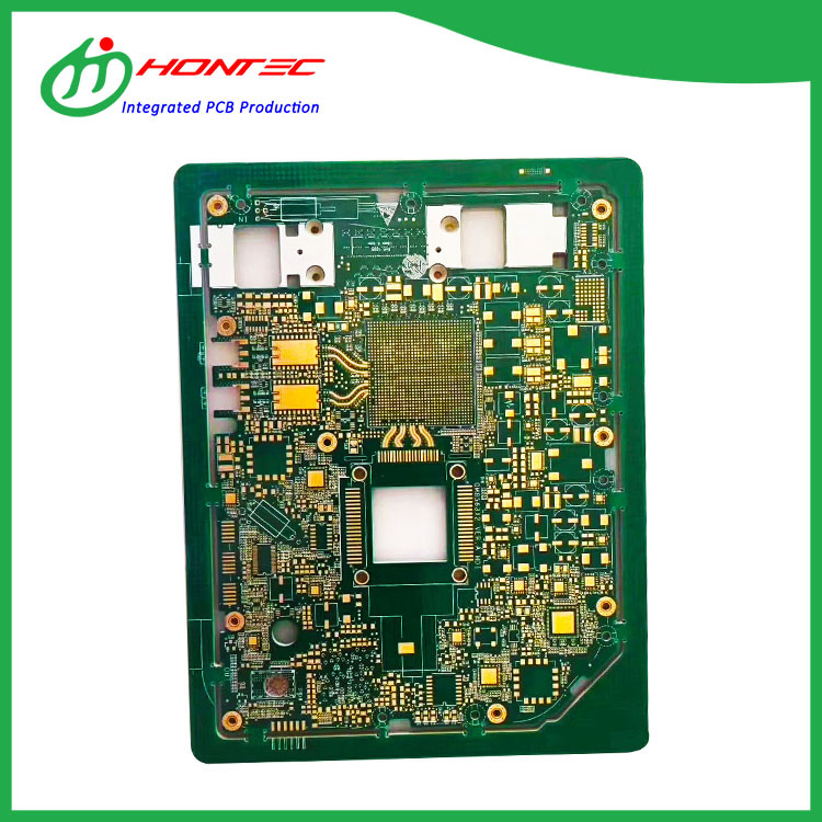
The TU-872SLK PCB is a circuit board produced by combining microstrip technology with lamination technology or optical fiber technology.It has a large capacity, and many original parts are directly made on the circuit board, which reduces the space and improves the utilization rate of the circuit board.The following is about TU872SLK PCB related, I hope to help you better understand TU872SLK PCB.
Read MoreSend Inquiry4 Layer High Precision HDI PCB
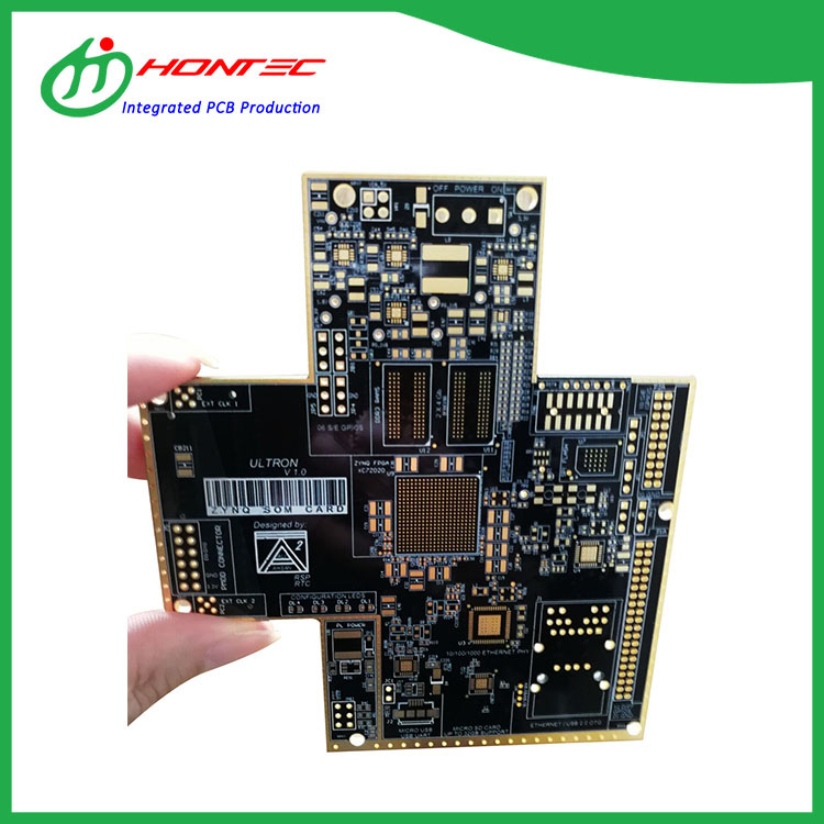
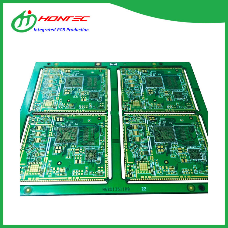
This kind of PCB with a whole row of semi-metallized holes on the side of the board is characterized by a relatively small aperture. It is mostly used on the carrier board as a daughter board of the mother board. The feet are welded together.The following is about 4 Layer High Precision HDI PCB related, I hope to help you better understand 4 Layer High Precision HDI PCB.
Read MoreSend Inquiry


