- Español
- Português
- русский
- Français
- 日本語
- Deutsch
- Italiano
- Nederlands
- Polski
- 한국어
- Svenska
- magyar
- Malay
- বাংলা ভাষার
- Dansk
- Suomi
- हिन्दी
- Pilipino
- Türkçe
- Gaeilge
- العربية
- Indonesia
- Norsk
- تمل
- český
- ελληνικά
- український
- فارسی
- български
- Latine
- Azərbaycan
- Македонски
- Lietuvos
- Eesti Keel
- Română
- Slovenski
- Srpski језик
- 简体中文
- Català
- שפה עברית
- беларускі
- Frysk
- ગુજરાતી
- ಕನ್ನಡ
- Kurdî
- Gàidhlig
- Тоҷикӣ
- O'zbek
- Lëtzebuergesch
Products
- View as
-

-

6-layers 2Step HDI PCB
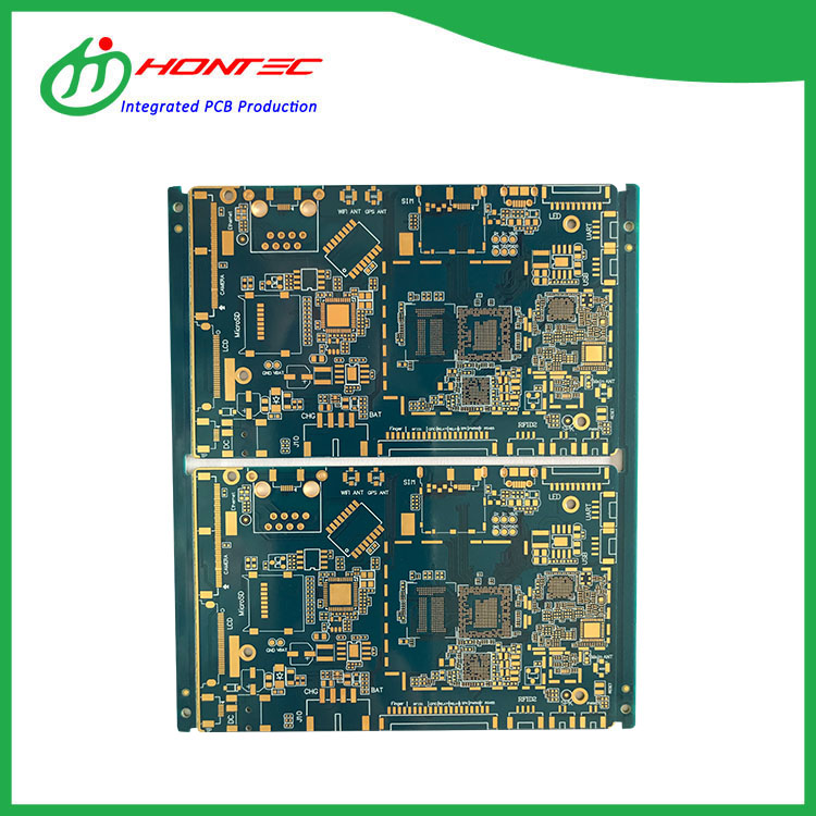
6-layers 2Step HDI PCB Laminate twice. Take an eight-layer circuit board with blind/buried vias as an example. First, laminate layers 2-7, first make elaborate blind/buried vias, and then laminate layer 1 and 8 layers to make well-made vias .The following is about6 layers 2Step HDI, I hope to help you better understand 6 layers 2Step HDI.
Read MoreSend InquiryIPAD HDI PCB
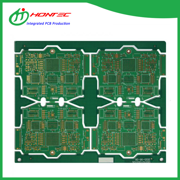
HDI is the abbreviation of High Density Interconnector. It is a kind of technology for the production of printed circuit boards. It is a circuit board with a relatively high line distribution density using micro-blind buried via technology.The following is about IPAD HDI PCB related, I hope to help you better understand IPAD HDI PCB.
Read MoreSend Inquiry18 layer 3step HDI PCB
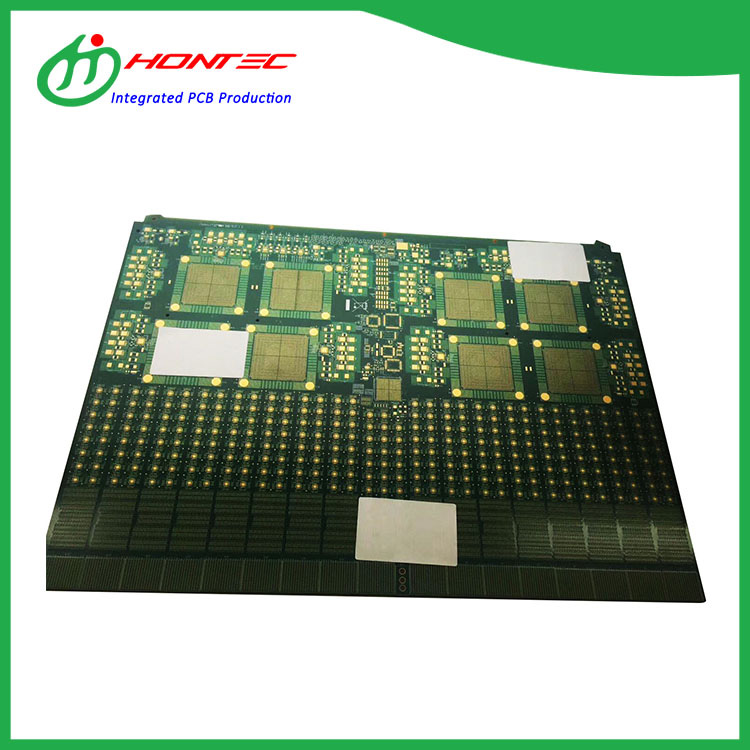
18 layer 3step HDI PCB refers to the HDI circuit board with more than 2 levels, usually 3 + N + 3 or 4 + N + 4 or 5 + N + 5 structure. The blind hole uses a laser, and the hole copper is about 15UM.The following is about 18 layer 3step HDI circuit board related, I hope to help you better understand 18 layer 3step HDI circuit board.
Read MoreSend Inquiry28-Layer 3step HDI PCB
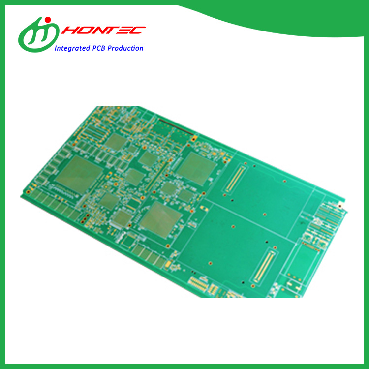
28-Layer 3step HDI PCB While electronic design is constantly improving the performance of the whole machine, it is also trying to reduce its size. In small portable products from mobile phones to smart weapons, "small" is a constant pursuit. High-density integration (HDI) technology can make the design of end products more compact while meeting higher standards of electronic performance and efficiency. The following is about 28 Layer 3step HDI Circuit Board related, I hope to help you better understand 28 Layer 3step HDI Circuit Board.
Read MoreSend Inquiry4step HDI PCB
4step HDI PCB is widely used in mobile phones, digital (camera) cameras, MP3, MP4, notebook computers, automotive electronics and other digital products, among which mobile phones are the most widely used.The following is about 4Step HDI Circuit Board related, I hope to help you better understand 54Step HDI Circuit Board.
Read MoreSend Inquiry


