- Español
- Português
- русский
- Français
- 日本語
- Deutsch
- Italiano
- Nederlands
- Polski
- 한국어
- Svenska
- magyar
- Malay
- বাংলা ভাষার
- Dansk
- Suomi
- हिन्दी
- Pilipino
- Türkçe
- Gaeilge
- العربية
- Indonesia
- Norsk
- تمل
- český
- ελληνικά
- український
- فارسی
- български
- Latine
- Azərbaycan
- Македонски
- Lietuvos
- Eesti Keel
- Română
- Slovenski
- Srpski језик
- 简体中文
- Català
- שפה עברית
- беларускі
- Frysk
- ગુજરાતી
- ಕನ್ನಡ
- Kurdî
- Gàidhlig
- Тоҷикӣ
- O'zbek
- Lëtzebuergesch
Products
- View as
-

-

Multilayer PCB
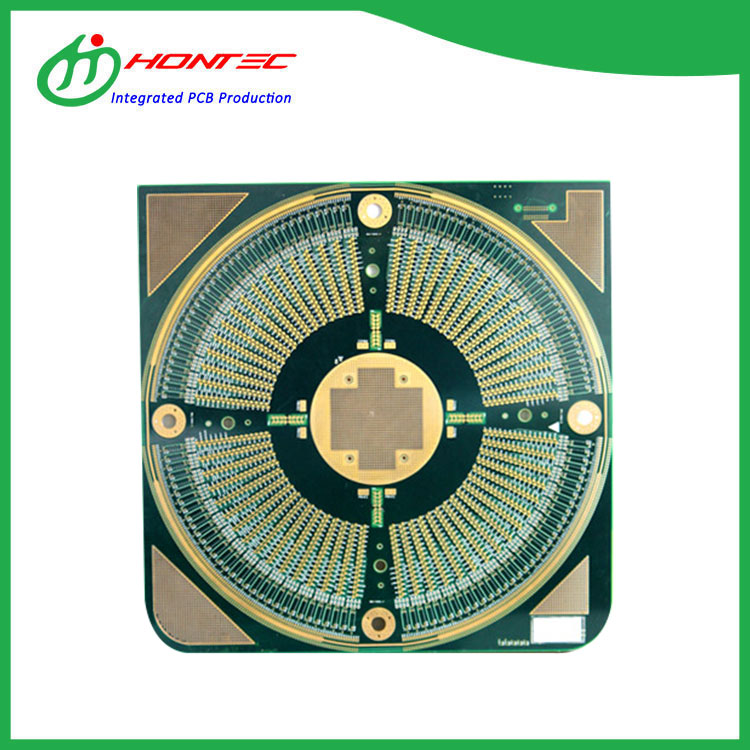
Multilayer PCB refers to a printed circuit board with more than three conductive pattern layers and insulating materials between them, and the conductive patterns are interconnected according to the requirements. Multilayer circuit board is the product of the development of electronic information technology to high speed, multi-function, large capacity, small size, thin and lightweight.
Read MoreSend InquiryStep Gold finger PCB
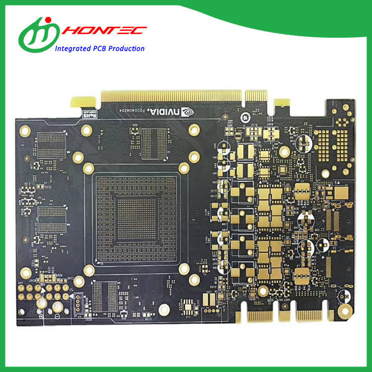
The golden finger is composed of many golden yellow conductive contacts. It is called "golden finger" because its surface is gilded and the conductive contacts are arranged like fingers. The step gold finger PCB is actually coated with a layer of gold on the copper clad laminate by a special process, because the gold has strong oxidation resistance and strong conductivity.
Read MoreSend InquiryMultilayer precision PCB
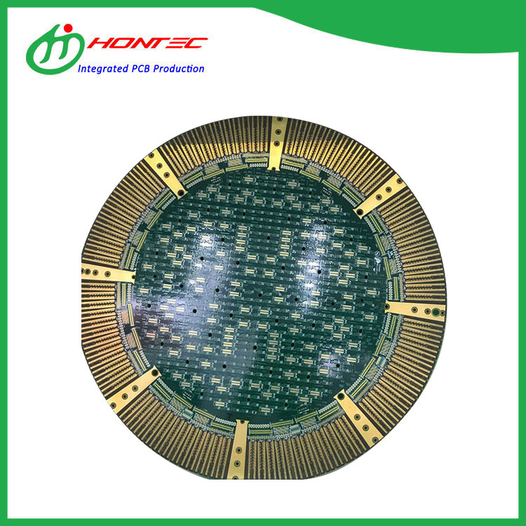
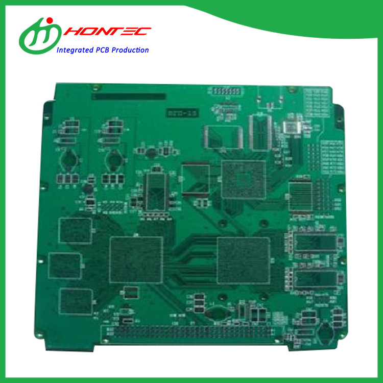
Multilayer precision PCB--The manufacturing method of multilayer board is generally made by the inner layer pattern first, and then the single or double-sided substrate is made by printing and etching method, which is included in the specified interlayer, and then heated, pressurized and bonded. As for the subsequent drilling, it is the same as the plating through-hole method of double-sided board.
Read MoreSend InquiryImpedance Control PCB
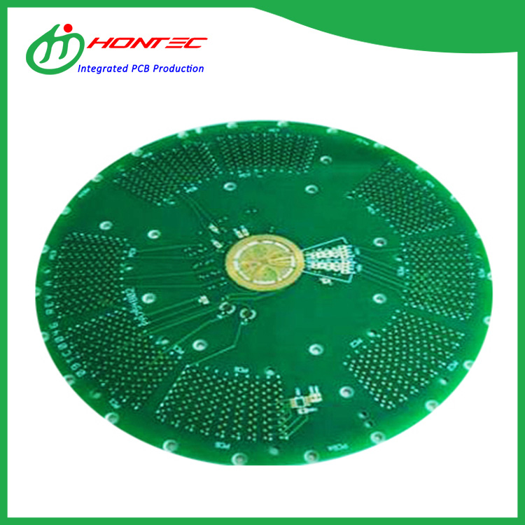
At high speeds, Impedance control PCB traces are used as transmission lines, and electrical energy can be reflected back and forth, similar to the situation where ripples in lake water encounter obstacles. Controlled impedance traces are designed to reduce electronic reflections and ensure correct conversion between PCB traces and internal connections.
Read MoreSend InquiryHard gold PCB
Hard gold PCB--plating gold can be divided into hard gold and soft gold. Because the hard gold plating is an alloy, the hardness is relatively hard. It is suitable for use in places where friction is required. It is generally used as a contact point on the edge of the PCB (commonly known as gold fingers).The following is about Hard gold plated PCB related, I hope to help you better understand Hard gold plated PCB.
Read MoreSend Inquiry


